


Allion USA-SGS
In our previous article, Analysis of and Introduction to Wireless Product Performance Improvement (I), we explained how antenna design and performance can affect results, specifically after the antenna is modified, the RX still indicates “fail” at the 2.4GHz band (100m distance). According to our research, we’re assuming the poor reception is due to noise interference. Therefore, we will first introduce the basic concepts of RF performance debugging and its practical applications, then we will explain what we have modified.
Noise Interference Causes
Noise Interference refers to unnecessary signals that the system generates which can affect its own performance. The following is a brief introduction to possible sources of noise interference and solutions.
First, you need to find and measure the source of the noise interference or where it’s leaking from, and this can be done with radiation, using a near-field probe (shown in the picture below). When the probe is close to the noise interference, the energy change of the frequency band can be seen from a spectrum analyzer.
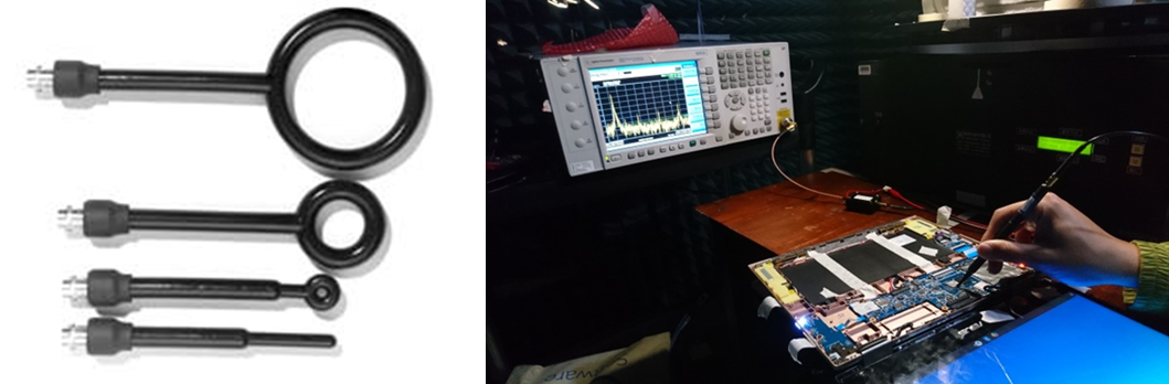
Near-field Probe (Left): Near-field probes are usually circular or rod-shaped. The circular probes are usually used for large areas and have different types of sizes, which can measure different areas and intensities of frequencies. The rod-shaped probes are usually used for small areas such as circuit board wiring and component pins.
Measurement Setup (Right): A complete testing setup consists of one near-field probe and one spectrum analyzer. However, adding a low-noise amplifier (LNA) can help amplify the interference, making it easier to read the information in the spectrum analyzer.
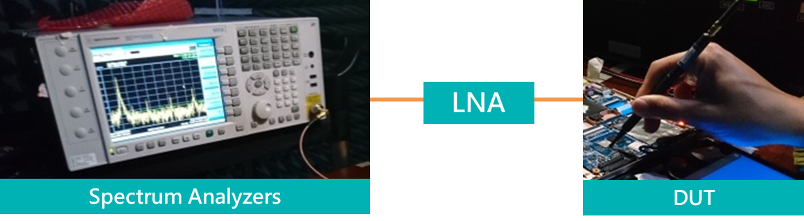
Adding a low-noise amplifier (LNA) will help amplify the noise energy, making the noise more obvious on the spectrum analyzer.
PCB circuits and mechanism design are the two main ways you can deal with noise interference. PCB circuits are relatively complex because there are lots of electronic components that may be the source of the interference. The interference can also get stuck within the product due to physical wire contact or high-frequency coupling.
PCB Circuit Noise Interference Debugging
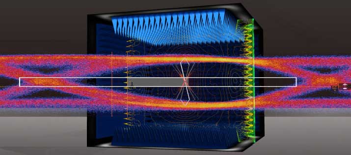
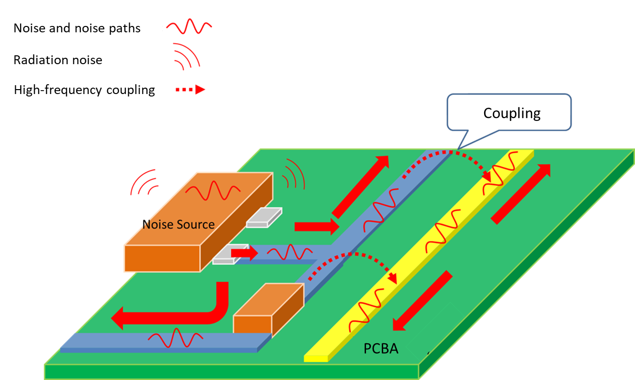
As shown in the picture below, the noise source transmits noise to other circuits through physical connections. High-frequency coupling is shown between the blue and yellow wire. Even though the wires aren’t connected, the yellow wire still gets affected by noise.
After having a basic understanding of the noise within a circuit, some difficulties or costs will increase when trying to decrease overall noise interference.
- Adding filter capacitors, common mode filters, or ground (large areas) will increase costs.
- If the circuit design is changed, the PCB board will need to be remade, thus increasing costs.
- If the circuit is more complex and the noise debugging isn’t done well, it will result in the modified circuit not being able to reach expected standards.
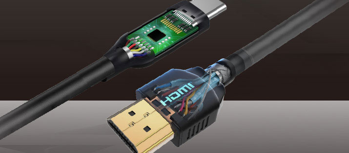
- If noise interferences come from necessary components such as CPU, memory, USB system chips, or high-speed circuits such as HDMI, it will be impossible to add capacitors, filters, or metal shields to them because it might cause problems for data transmission or heat dissipation.
There are lots of limitations when debugging circuits, so fixing the problem in mechanism design would be much easier. A good mechanism design can achieve good results without modifying the circuits.
Mechanism Design Noise Interference Debugging
There are several methods for getting rid of interference with mechanism design, for example using a metal shield on the PCBA, the components inside the chassis, and the outer components. Some examples will be explained below.
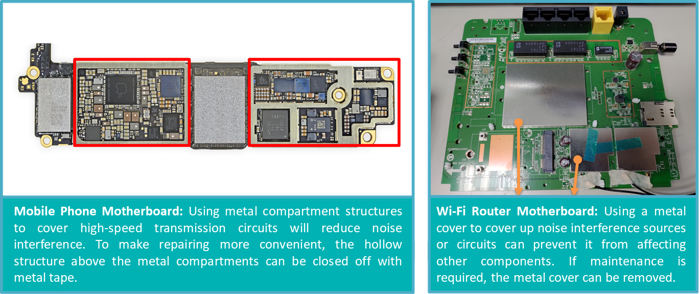
Metal Shield for the PCBA
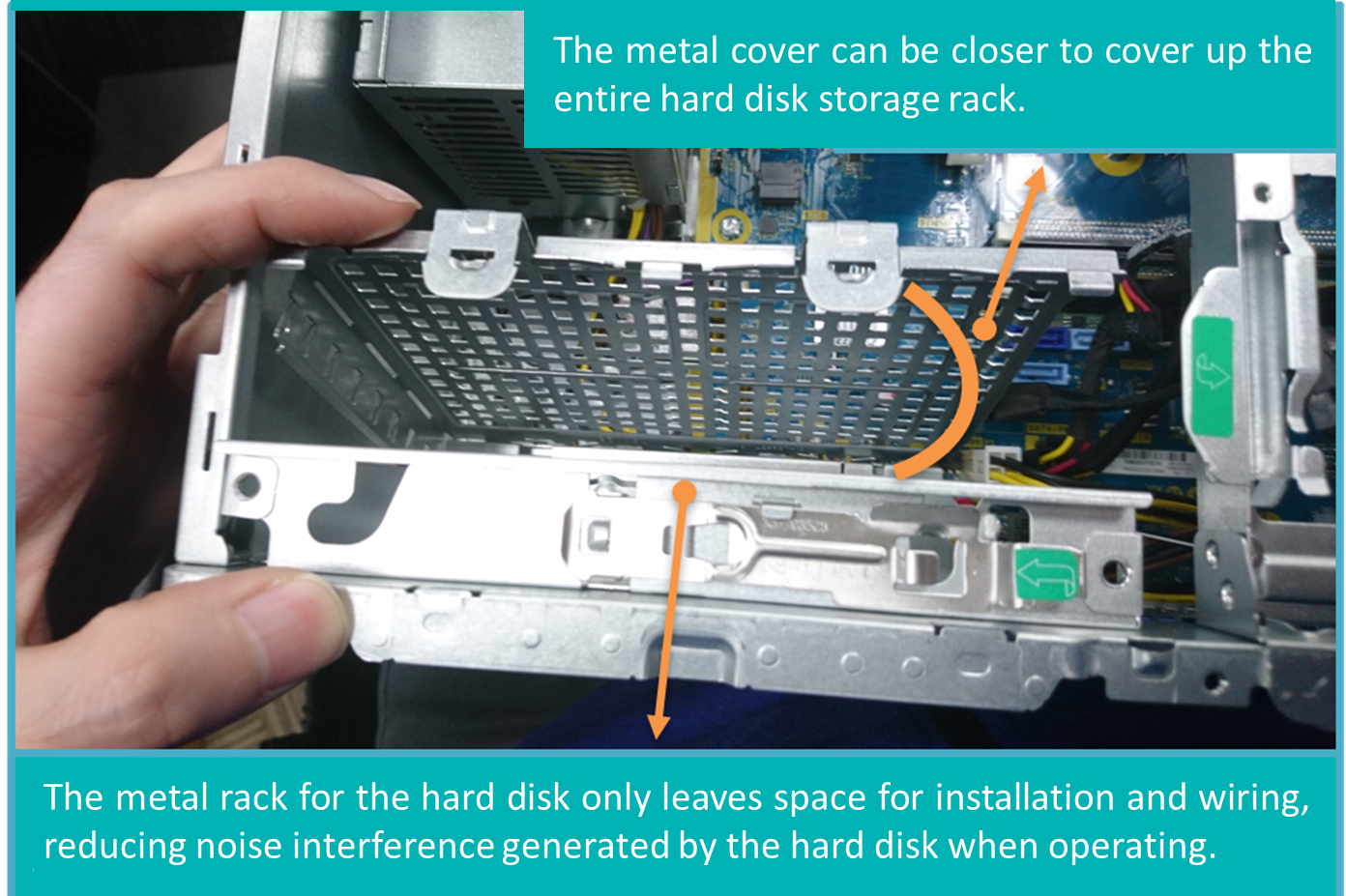
Internal Components of a Chassis
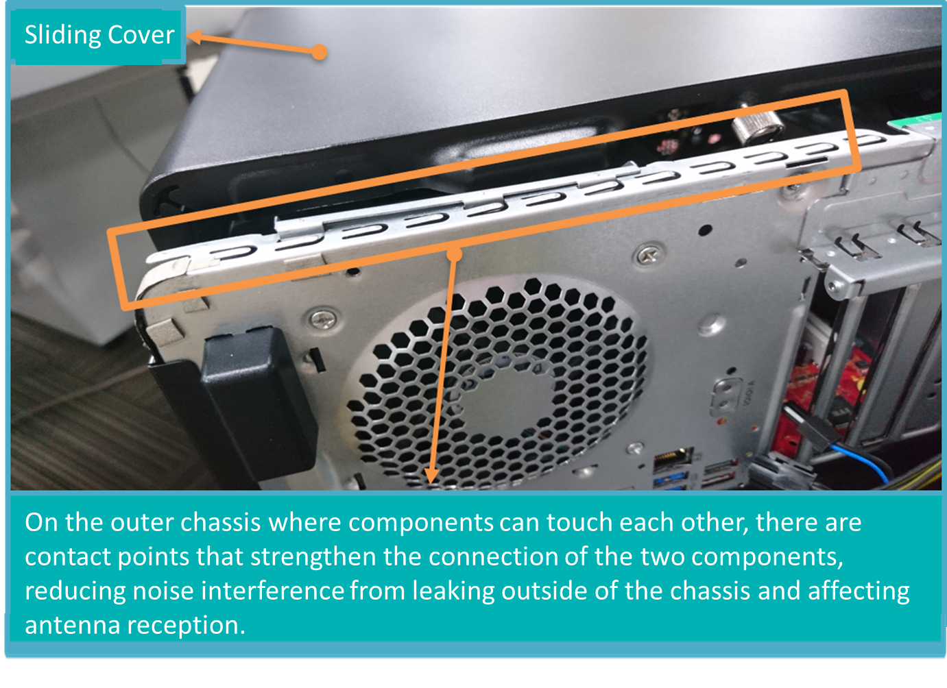
Outer Components of a Chassis
Noise Interference Solutions
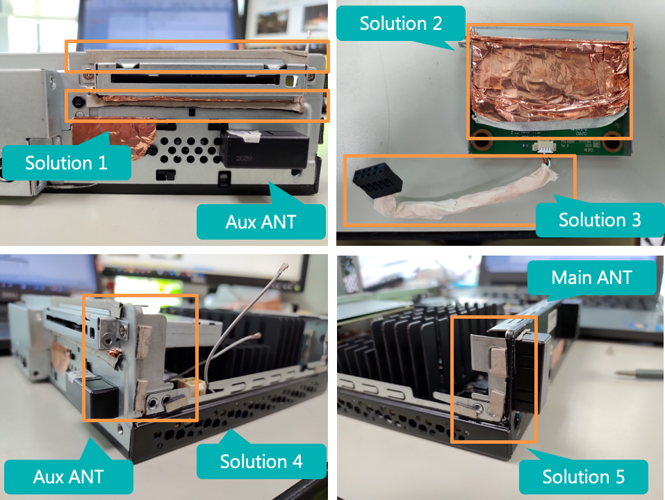
Referring back to the case at hand, let’s see how we can decrease noise interference based on the knowledge we learned above. Since the positions of the antennas have been changed to one in the front and one in the back, they should be treated independently. With an RF probe and a spectrum analysis, we can find out where the noise is leaking and come up with a solution to deal with it, as shown in the pictures below.
| Solution | Description |
| Solution 1 | Use metal tape or conductive foam to strengthen the overlap between the card reader and the chassis and reduce the gap, decreasing the leakage of the noise interference inside the chassis that affects the front antenna (Aux ANT). |
| Solution 2 | Cover the body of the card reader with metal tape and reduce the noise interference coming from the PCBA on the front antenna (Aux ANT). |
| Solution 3 | Cover the wire that connects the card reader with metal tape to reduce radiation noise. |
| Solution 4 | Add conductive foam between the chassis and the sliding cover, reducing the impact of noise leaking to the front and rear antennas (Main ANT and Aux ANT). |
| Solution 5 |
Here are the graphs from the spectrum analyzer after using the solutions above.
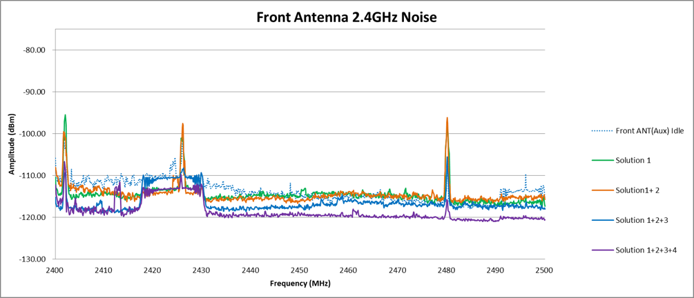
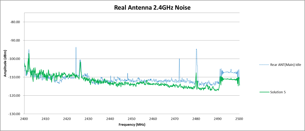
After noise debugging, the noise intensity of the front wall antenna was reduced by roughly 8dB and the rear antenna was reduced by 3dB, meaning these solutions are effective in getting rid of noise interference. A throughput test can be performed next to confirm the impact of our solution on the antennas.
| Frequency Band | Bandwidth | Channel | Spatial Stream
(TX/RX) |
20m Distance (Mbps) | |||
| SPEC | Two Front Antennas
(Original Version) |
One Front Antenna
One Rear Antenna |
One Front Antenna
One Rear Antenna (After Noise Debugging) |
||||
| Test Result | Test Result | Test Result | |||||
| 11n 2.4GHz | HT20 | CH1 | RX | 70 | 27.73 | 74.07 | 92.77 |
| CH11 | RX | 70 | 34.88 | 59.65 | 92.00 | ||
| HT40 | CH11 | RX | 110 | 50.63 | N/A | 185.18 | |
From the table above, adjustments to the antenna position and noise reduction are done incrementally, where we can observe the RX throughput for 20m distance continually improves, proving that our debugging methods are effective.
| Frequency Band | Bandwidth | Channel | Spatial Stream
(TX/RX) |
100m Distance (Mbps) | |||
| SPEC | Two Front Antennas
(Original Version) |
One Front Antenna
One Rear Antenna |
One Front Antenna
One Rear Antenna (After Noise Debugging) |
||||
| Test Result | Test Result | Test Result | |||||
| 11n 2.4GHz | HT20 | CH1 | RX | 40 | 9.20 | 19.44 | 34.89 |
| CH11 | RX | 40 | 8.20 | 19.69 | 34.16 | ||
| HT40 | CH11 | RX | 40 | 22.95 | N/A | 75.27 | |
The table above shows a throughput test of 100m. An improvement in throughput can be seen, but the HT20 CH1 and CH11 still cannot reach the SPEC requirement of 40 Mbps. As mentioned above, various debugging methods do not mean that the expected goal can be achieved. However, in a practical situation, a distance of 100m is already quite a long distance and the RX is still maintaining a steady throughput, meaning that users will not be able to tell the difference between these tiny changes in their usage.
In this case, our client considered the cost of debugging methods, market competition, and user experience before finally choosing our proposition, leading to a successful product launch. This means that Allion USA-SGS successfully helped them finish by taking into consideration the final effect, costs, and feasibility of their product.
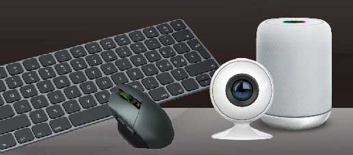
In recent years, there have been more and more IoT products popping up in the market and many electrical appliances now have wireless functions for communication, control, and other functions. Generally, small-scale companies or companies that are new to RF may not have related engineers to deal with noise interference issues. Allion USA-SGS has RF-related experience and can provide those services. With the methods mentioned above, we can assist our clients to solve these problems during each stage of your product launch.